Anycubic Photon PCB exposing Jig
thingiverse
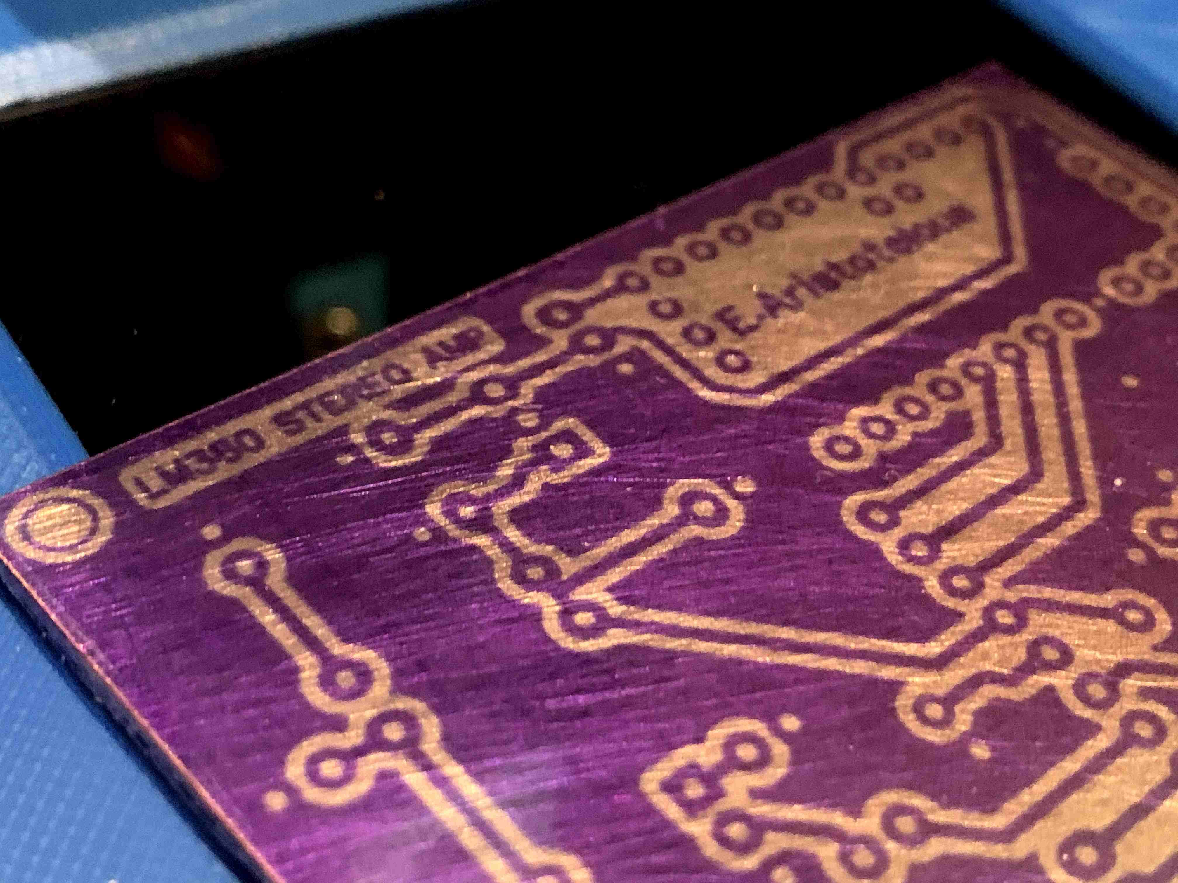
This is a quick jig I designed to hold 50x70mm copper clads with photoresist film applied to expose my designs using the Anycubic Photon. This technic yields very detailed results with some practice and cuts out the need for transparencies and other methods of exposing the PCB. You just need to print it, place it inside the printer instead of the vat and screw it in place. It should align itself and leave you with a square of exposed screen. Software-wise you will need to convert your PCB design to an STL so it can be sliced for the photon. I used 3D Builder on windows and Blender, but I am still figuring it out. Then you insert the STL to Photon workshop or other slicers and center the object. Slice with a bottom exposure time of around 6-8 minutes and load it onto the machine. After placing the PCB, photoresist down, run the file and after the time has passed you can retrieve your expose PCB. Etch and voila! I am still learning and trying to perfect my technic but I have made some pretty nice boards. I will add other sizes of jigs for common copper-clad sizes soon.
With this file you will be able to print Anycubic Photon PCB exposing Jig with your 3D printer. Click on the button and save the file on your computer to work, edit or customize your design. You can also find more 3D designs for printers on Anycubic Photon PCB exposing Jig.