CHIP, The 9 Dollar Computer
thingiverse
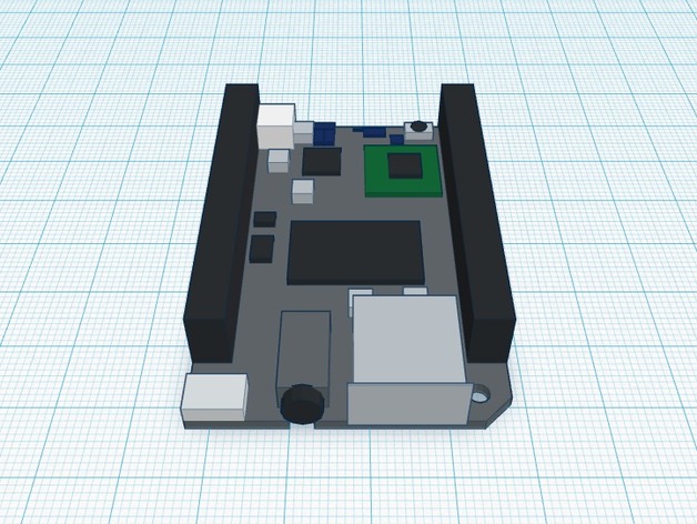
This is a model of CHIP The Nine Dollar Computer for you to use when building models for CHIP cases or accessories. It is not intended to be printed. I want to design some cases for CHIP and I usually model a subject before I model accessories for it. Until I had the CHIP board in hand, I couldn't design a case because I didn't know its exact dimensions. I'm sharing it for everyone else who might want to build accessories for CHIP. Now that I have modeled it, anyone should be able to make a case for it very easily. Model dimensions were measured in 1/10 mm intervals. I have seen several revisions of the board on the CHIP website. I assume that my board is the final production design and there are no other versions of it in the public's hands. If someone finds that is not the case, please let me know in the comments! Case Design Notes One of the challenges in building a case is knowing the contact points where you can apply pressure without damaging any components. CHIP employs some of the tiniest surface-mount electronic components around. There are so many and they are so hard to see and they are so dense that even if you can be sure you've found a spot free of components it would be so small that you may not be able to produce a case with enough precision to utilize it. Any inaccuracy could result if damage to a nearby SMD. I could never accurately model all the tiny components on the CHIP board. Never. Instead, I just marked the entire board blue (indicating sensitive components and therefore off-limits and made note of the following exceptions, which should be safe for contact with the case: The single screw mount hole in the corner next to the USB port and its surrounding copper pad, obviously. The four side edges of the circuit board (not the top or bottom surfaces, just the thin side edge). The top of any peripheral connectors on the edge of the board (USB, micro USB power, composite video, JST-PH battery socket, I/O header sockets, if not being used). Excessive pressures may deform sockets and prohibit operation, especially the JST_PH socket. It's best to have contact pressures on the BACK of the socket, rather than the front. The top and bottom of the IO header sockets (the long, tall black rows). The red zones indicated in the uploaded images of the model. The pins of the headers did not appear to be soldered, but rather compression-fit into the vias. I worry that too much pressure on the bottom of the header pins and any downward pressure elsewhere may cause the header connection to become unreliable or even cause the header to pop off the board. Be sure to put opposing downward pressures on the top and bottom of the IO header to avoid this. If you expose the I/O headers, it's best not to put any pressure below them. Because STLs don't support color, I have provided the two screen shots of the top and bottom of the model before exporting to STL. The first is an actual model of the CHIP. The second has blue regions to indicate off-limits areas occupied by SMDs and red zones to indicate possible safe zones for contact. Because STLs don't inherently support color, I have raised the blue and red zones by 0.1 mm so that you can see them in the model. You'll have to refer to the photos to figure out what each zone's color is, unfortunately. If anyone has a better idea about how to handle this, please leave a comment. Legend Color scheme: Orange / gold are bare metal copper pads, through-hole pins or other electrical contact exposure. Dark gray are silver or chrome colored connectors Light gray are large protruding components (inductors). Dark blue are various surface mount components. Height may vary but most are 1mm or shorter. Most of the blue region is a careless blanket but I was very careful to model them accurately near the back edge and near the red zones. Green is used when modeling the RealTek slave board. It is actually green on the CHIP mainboard with a black RealTek package on the top so those are the colors I used. Black are semiconductors. Many of the small ones appear to be transistors, FETs or power regulators. The larger ones are memory, CPU, or other components. I've modeled every single one of these so that you know where they are for heat considerations when building a case. You'll know where someone might put a heatsink or where airflow may be most important. However, I don't know which of these chips will have a tendency to get hot, so that's for you to worry about :)
With this file you will be able to print CHIP, The 9 Dollar Computer with your 3D printer. Click on the button and save the file on your computer to work, edit or customize your design. You can also find more 3D designs for printers on CHIP, The 9 Dollar Computer.